Following my research for the previous article about the performance of SD/CF/USB flash modules, the only conclusion I could reach is that most of them are pretty dire. The only notable exception among the SD cards seems to be the latest generation of the SanDisk Extreme Pro (95MB/s) cards that just about managed to squeeze out enough performance on random writes to match a 7200rpm disk. Still, this is pretty dire compared to any reasonable SSD, so I wanted to see what else could be done about installing extra storage with good performance into a Toshiba AC100.
What I came across is this: SuperTalent RC8 USB stick. It may look like a USB stick, but it is actually a full-on SSD, featuring a SandForce 1200 flash controller. I figured this was worth a shot, even though the specifications indicate it is rather large (far too large to fit inside an AC100 in it’s standard form). Stripped out of the casing, however, it looks like RC8 might just be fittable inside the Toshiba AC100.
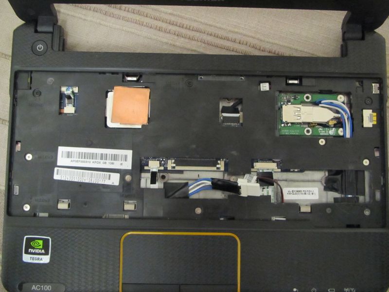
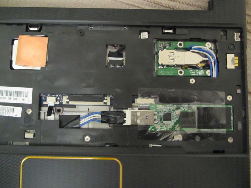
This is what I ended up with. There appears to be only one place inside an AC100 where a bare RC8 circuit board could be fitted. You will need the following:
1) P3MU mini-PCIe USB break-out module
3) Custom made USB cable (male and female type A USB connectors, some single core wire, and some skill with a soldering iron)
Measure out exactly how long you need the cable to be – there is no room to tuck away excess able inside an AC100. Here is what my cable layout ended up looking like.
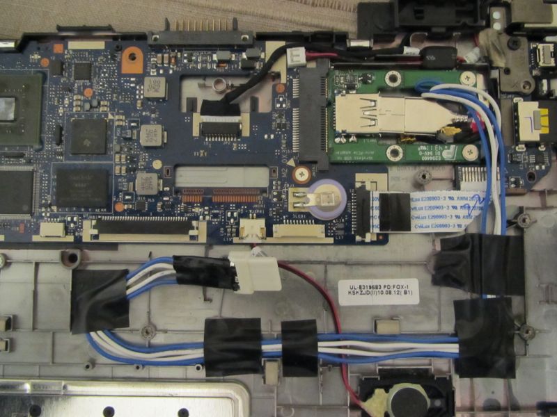
This is what it looks like with the top panel fitted. Note the large cut-out that has been made below the mini-PCIe slot access hole.
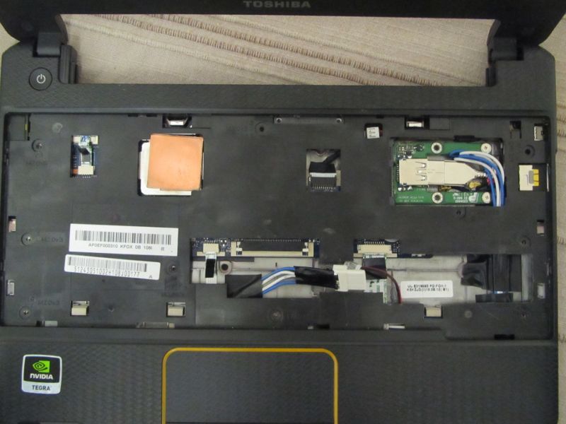
And again with the screws fitted. Note that one of the screw holes is in the area that had to be cut out. This shouldn’t affect the structural integrity of the AC100, though. Also note that the right speaker cable has been re-routed slightly to now go over the LED ribbon cable.
This is what it looks like with the RC8 attached. Now you can see why the cut-out in the top panel was exactly the shape it was – I specifically cut out the minimum possible amount to allow the RC8 to fit.
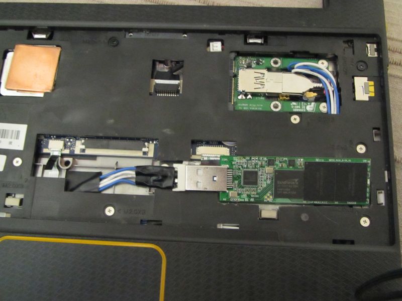
I also put a piece of thin transparent sticky tape over it to hold in in place, just to make sure nothing can short out against the underside of the keyboard.
And that is pretty much it. Put the keyboard back in and bolt it all together. The metal part of the USB connector will sit a tiny bit above the line of the panel, but the only way you’ll notice it once you put the keyboard back on is by knowing that there is a tiny bulge there.
Your AC100 should now be able to handle ~ 2000 IOPS on both random reads and random writes, along with much better life expectancy that having proper flash management brings.
At this point I would like to point out just how impressed I am with the SuperTalent RC8 USB SSD. Not only is the performance fenomenal (especially for a USB stick), but it really behaves like a SATA SSD – to the point where you can use tools like hdparm and smartctl on it (yes, it even supports SMART).


Sweet!
Now is there any place left inside that could be used to hold a tiny USB hub and a 3G modem? xD I have to admit – the integrated modem is the killer feature of the AC100 for me
.
And couldn’t you just cut out the top metal part of the USB slot? It’s not like it’s needed to hold the plug in
.
I very much doubt you could squeeze enough space somewhere to put a USB hub. The problem is that the USB connectors, especially the female end, are big. In the photos above, you’ll see that I actually removed the metal casing on the cable where the RC8 is connected – it’s the only way it can fit.
I don’t really see the integrated modem as that big a deal – most custom Android firmwares support tethering.
Well, I don’t own a smartphone, and don’t plan buying one. I’m almost happy with my 6-years old el-cheapo phone (Nokia FTW!) – except that it has too many features that clutter the interface. I wish someone did a phone that does nothing except calls, texts, and alarm clock. With a decent screen that can hold an entire SMS with a small font.
Well, enough of the off-topic
. I hope you now understand my stand on the modem.
Yes, fair enough. In that case you could solder the USB cable that goes to the RC8 directly to the second mini-PCIe header.
Is that second header-to-nowhere wired-up the same way as the first one (i.e. only USB)? Have you tried if it works correctly?
I haven’t tried it, but I think it is wired up the same way as the other one.
Screw connectors! Remove ‘em and solder the cables directly to the hub PCB. It’s not like you would disconnect them again, the hub was supposed to become a part of the smartbook.
But if the second PCIe header really has the USB lines wired as you said, all this is obviously not needed.
And you could do a few benchmarks to check if zram is still worth the hassle. I can imagine with that kind of IOPS it could be faster to just swap directly to the SSD…
It probably is, but it means needlessly wearing out the flash.
Then again, the 25GB RC8 actually has 32GB of flash on it – it is over-provisioned by 7GB, to enable some seriously advanced wear leveling and defect management. So in fairness, the chances of actually wearing out this SSD in any kind of sane use any time soon are pretty remote.
They’re even more remote if you shell out on a larger disk. The nice thing with SSDs is that the endurance is proportional to capacity!
Then again, the 100GB SuperTalent costs over twice as much as the AC100 itself. LOL.
It’s not just about size – it’s also about over-provisioning. With 7GB of space to play with on a 25GB disk (or 28 on a 100GB disk), you can do a LOT of clever flash management behind the scenes, that gets the write amplifications down to 1, or even lower if your controller also happens to do compression and deduplication (which the SandForce controller is rumoured to be doing).
I never claimed it’s not. This doesn’t change the fact that with a fixed amount of write cycles per block, a drive with twice the number of blocks will survive twice the total number of writes, ceteris paribus. At least with really good wear leveling.
That said, 28% of over-provisioning is really impressive. With all the good things you hear about SandForce, any of those drives is probably going to survive a long time used as a swap drive.
And if it doesn’t, at least you don’t have to solder anything to replace it with a new one
.
Hi,
Congratulations for your work with Toshiba AC100. I’m getting a lot of ideas and want to begin to squezze my AC100.
I have the 3G version, and I’m really interested to not remove 3G module…
Looking some solution, I find an express card with two USB ports, so maybe I could have a 3G module in one of them and the other one with any large storage option.
This is what I have found
Mini PCIe USB 3.0 Card 2 Port NEC CHIP
This card is suitable to be installed in our Toshibas?
Since you haven’t listed a source or part number for the card I cannot take a look at how it actually works. Unless the card is a simple USB hub it wouldn’t work, since the mini-PCIe slot doesn’t actually have the PCIe lines wired up, it only has USB.
What you could do, however, is wire the USB lines for the USB stick by soldering them onto the 2nd mini-PCIe header that is on the motherboard. The second slot isn’t soldered on, but the USB lines might be wired up to it. That would allow you to fit the internal USB SSD without sacrificing the 3G module.
Hmm. This brings the question whether the second header is wired-up and how (I’d fall off the chair if you told me it has only PCIe wired with no USB
). Could you run “lsusb -v” as root on your AC100 and post the output here? It could give us some clue about the internal USB layout.
Sure, here is the output of lsusb -v.
Hmm, that is odd.
According to that listing, that device has two single-port root controllers laid out like this:
Root 0:
– 2-port hub
– WiFi controller
– Bluetooth controller
Root 1:
– 3-port hub
– Ericsson 3G modem
– Camera
– SCSI mass storage
As it comes, there is not a single unplugged port here. What kind of AC100 is it, and what devices were connected when you made that listing? I’m assuming it’s an unmodded unit, as the 3G modem is still there
.
Indeed, that lsusb dump was taken on a completely unmodified AC100-10U. The SCSI mass storage device is an external USB disk.
This doesn’t look good. As every single port is used, It looks like there isn’t any additional USB line on the second mini PCIe connector. Oh well, seems like I’ll have to go the hub way. Lots of soldering to do on the horizon…
PS: Yeah, I finally bought an AC100-10E yesterday. I expected Android to be really bad on this device, but… it’s much worse than that. No wonder this toy didn’t sell well for Toshiba.
In case somebody here is interested, some guy is trying to sell an AC100-10K with a broken screen for 300PLN (~£60) on a Polish auction site Allegro. Sounds like a nice deal if you plan to replace the screen anyway
. No 3G and no BT on this particular model is a deal-breaker for me, but maybe somebody…
.
Dang, these SuperTalent sticks are expensive! For the price of a 50GB one I could get a 120GB OCZ Vertex 3 SSD for my desktop and a few beers. Where do they get customers willing to pay that much? It’s not like there are that many AC100 modders out there
your article is amazing, but i have a few questions:
1) what difference does it make, between your “internal” rc8 and a rc8 inserted externally?
2) can i use a mini-pci-e ssd card instead, would that work?
1) Inserting it externally means you are using up the only external USB port.
2) I suggest you read part 1 of the article, it explains why you cannot use a normal mini-PCIe SSD.
Do you have any photos of the rear side of the motherboard? I’ve just been staring at the schematics for a little while, and I’ve come up with a cunning plan to provide two or three more USB ports on a fully-loaded AC100 without your WWAN hack. But I don’t actually own an AC100 (yet), so I’m guessing a bit!
According to the circuit, U9 is an SMSC USB2514B USB hub chip that gives 4 USB ports (WWAN, webcam, external USB and SIM card) on Tegra’s USB port 3. U10 is a USB2512B that gives 2 ports for Wifi and Bluetooth on Tegra’s USB port 2. (Tegra port 2 isn’t native from the SoC like the others, it uses a USB PHY chip which is a USB3315. Tegra port 1 is the mini-USB device port)
Evil hack #1 is that port 4 on U9 appears to be wired to the spare pins on the SIM card. This is part of recent SIM card standards, but I don’t think anyone uses it (never seen an app for reading your contacts off the SIM this way, for example). So that port could be pinched. I don’t have a detailed enough photo to see how this might work physically.
Evil hack #2 is that the footprints for the USB2512(B) and USB2514(B) are the same pinouts. And the pins for ports 3 and 4 of U10 aren’t connected to anything. So if it’s replaced for a USB2514B (about £3 from RS) and add four more wires you get an extra two ports to play with. The QFN36 package is small, but not unmanageably small if you have a hot air soldering system.
In other news, I had a look at a RAM upgrade which sounds feasible if the right chip exists (if there’s a clean 512Mb x 8 DDR2 chip out there it should work, but I can’t find anything without odd banking arrangements) and the firmware problem is sorted. Would also need a bodge wire to provide A14 to each DRAM chip, and I think the relevant ball is on the edge of the Tegra so accessible. But all a bit extreme.
And I spotted a crazy thing on the schematic… there’s an empty NAND flash space (U25)… but none of the address lines are wired, only the data and control lines. So there’s no way to address more than 1 byte of memory!
And another interesting finding… JMIN1 (the mini PCIe slot with a bar of PCB across it that holds the ribbon cable for wifi and Bluetooth connections – presumably which can be snapped off) is wired to Tegra’s SDIO port 2. So, assuming the kernel knows to probe this port, a microSD or maybe even full SD card could be fitted in here to coexist with the wifi bar without too much pain…
(schematic is here by the way:
http://hobi-elektronika.net/toshiba-ac100/
I used Ghostscript to convert to Postscript to get rid of the password protection)
I have two AC100-W machines with (16G, WiFi, 3G, no BT) and one AC100-N (32G, WiFi, no 3G, no BT). One of the 3G machines is without display and with some damage to the plastic (this is going to be headless compile station and source of spare parts), so i’ve stripped it down and will take some photos of internals if somebody is interested. Those with displays are running 3.x kernel (built for Ubuntu Precise Pangolin), but the userspace is gentoo hardfloat, compiled locally, running on the SD card. So far this is my unsorted list of findings / thoughts:
- USB port connected to SIM isn’t showing up anywhere. Even with SIM card inserted there is no new device detected / listed. I think these are connected, but can’t find a way to check this from within linux.
- Accelerometer BMA150 (chip U16) is missing
- Ambient Light Sensor ISL29011 (chip U17) is missing (there isn’t even hole in the case/body to allow light in – sensor should be somewhere between ESC key and power button, but there is a hole in the powerbutton pcb, so drilling very thin hole to the case should do the job)
- TPM module ST19NP18ER28 (chip U26) is probably missing (haven’t checked bottom side yet, can’t find U26 mark on the top side)
- NAND memory (chip U25) is missing (as noted by Theo and other sources), but it should be working if added. This NAND memory (NAND01GW3B2AN6F – 1Gbit/128MByte) supports data/address multiplexing, thus data + control lines are all what is needed (you can even instruct bootloader to boot from NAND instead of eMMC/SD)
- JMIN1 (mini-pcie type connector for WiFi/BT) supports SDIO+UART only, datasheet links to this particular card – UHMC-(A)GNB-AR-01 (SDIO WiFi / UART BT combo). As there is a JP2 connector on the “bridge” in my ac100w, which prevents any card to be present (if the connector would be soldered), it looks like design option to support either WiFi+BT combo in the mini-pcie or an USB WiFi(+BT) in the JP2. The occupied “bridge” is visible in the photo here: http://wiki.gudinna.com/uploads/768/11b.CIMG0231.JPG . This means there is possibility to have both WiFi+BT + 2 spare USB ports (but you have to find some SDIO WiFi / UART BT -these are RARE- and do some careful soldering)
- JP2 (USB WiFi/BT connector) is fully populated on the AC100W, even the cable is fully connected, but this version has only WiFi. This means one port ends somewhere “in the void” on the MS-3822 WiFi pcb. For some strange reason one pin is named “BT_WAKEUP” and one “WF_PWDN”. It looks like power switching is shared for WiFi and BT.
- JMIN2 (mini-pcie type connector for WWAN/3G) is present on ac100w (obviously) and equipped with Ericsson F3307 (3G) module. This is stripped down version of F3607gw (3G+GPS) module and according to all sources these two are pin-compatible (GPS “should” be multiplexed as an extra ttyACM port, not connected to extra pins – there are no other datapins wired on the ac100 side). I’m planning to obtain one of the GPS enabled ones in near future for the test.
Now some questions / requests:
- Can somebody upload a picture of the WiFi+BT combo adapter (it’s the small pcb next to the camera in the upper left corner of the display frame) or post some extra details?
- Is it possible to switch off BT / WiFi independetly on the USB-WiFi/BT enabled units, or are these two switched on/off at the same time?
- Has anybody seen a machine with second mini-pcie slot fitted/equipped? (or were these only pre-production units or small series, as it looks there are no commonly available SDIO cards in mini-pcie form factor)
Links / etc:
UHMC-(A)GNB-AR-01 – http://www.bluetooth.com/Pages/Product-Listing-Detail.aspx?ProductID=13680 – looks like some reference card, isn’t mentioned anywhere else, only on ARM related sites / datasheets – AC100, i.MX53 etc.
W2CBWG03 – http://www.mouser.com/access/?pn=648-W2CBWG03 – another candidate for JMIN1 card (SDIO WiFi +USB BT. W2CBWG01 is GPS enabled. Schema lists BT interfaces on both as USB/UART/SPI/GPIO, but then it’s listed as USB only – weird)
Ericsson F3307 datasheet – http://www.ericsson.com/solutions/mobile_broadband_modules/docs/F3307_screen.pdf
Unfortunately I don’t have any photos of the underside of the motherboard. I’ll try to remember to get some next time I have a reason to open up one of my AC100, but it may not be any time soon.
Fantastic bit of research on the extra USB port possibility, as well as bigger RAM chips and an SDIO port.
Another question… have you tried using your USB stick as swap? How well does it behave?
I’ve been doing some more evil thinking regarding increasing the RAM…
First up, I was getting confused. The NAND flash slot is indeed is correct in not having an address bus – it’s NOR that’s addressable, for NAND you have to go through a multiplexed interface (you write the address as 5 byte-wide transfers). So it should be possible to drop a standard NAND chip in there (there appear to be Tegra 2s using 4GB NANDs at least).
The NAND interface is actually fairly clean, and it might be a neat way to put extra RAM into the system – - make something that looks like NAND but is actually RAM. Trouble is, I had a look at this and the messy thing is the RAM side of it. Even though we want it slow (all has to go through the 8-bit NAND interface which is about as quick as the memory bus on a 386), to get a decent size of RAM means DDR or DDR2 and these are a pain to drive. That means squeezing a big FPGA and a SODIMM in there… not easy.
But an alternative plan is just to drop a fast NAND flash in there. Potentially it’s going to be quicker than USB due to lack of protocol overhead. Particularly an SLC NAND that’s optimised for minimising erase times (which is what really kills, and seem to vary between 1.5 and 3.5ms). The trouble with NAND is block wear, since there’s no translation layer, but a flash file system could help this (especially if the NAND is much bigger than the swap size). Actually, a decent layer designed for using NAND as swap might do quite well – do wear levelling, have 2-4x as much flash as swap, fire off erases whenever things are quiet and a page becomes deallocated rather than when the space is needed right this minute…
Perhaps I should stop thinking up crazy ideas
On the other hand, a fast NAND could be soldered in without too much pain, then throw it at JFFS2/YAFFS/etc (make a big file, mount it loopback, then use the loopback device for swap) and see what happens…
Looks like’s someone’s already written my magic Linux swap-on-flash driver (click ‘view by thread’ to see the rest of the patches):
http://lists.infradead.org/pipermail/linux-mtd/2007-March/017595.html
Aha, it finally made it into mainline Linux last year – /dev/mtdswap – see here for kernel options:
http://lists.infradead.org/pipermail/linux-mtd-cvs/2011-March/007193.html
I think I can see some fun coming up
Aw, crap. I just bought a fast SD card to install my system on – at least until I manage to do the SSD mod. I just put it in the reader slot, and… WHY DIDN’T ANYBODY TELL ME THE CARD DOESN’T FIT ENTIRELY INSIDE THE SLOT!?!?!? Why didn’t I bother to check it myself? ;_; This is just awful. I think I’m going to get drunk today. *bangs his head on the wall*
Hi,
what do you think of throwing the tegra 2 inside the ac100 away and build the odroid-x exynos 4412 plate in? Would that be possible?
tech data:
CPU Module Exynos4412 Quad Core CPU module
LAN/USB Hub LAN9514 4-port Hi-Speed USB 2.0 hub and 10/100 Ethernet controllers from SMSC
Audio CODEC MAX98090 is a full-featured and high performance audio CODEC from MAXIM
DC/DC Converter RP505K331B for 3.3Volt system power supply from RICOH
Level shifter FXMA2102L8X for I2C/UART/HDMI voltage translator from Fairchild semiconductor
Camera (Option)
S5KECGMIPI 2-Lane camera interface on rear side from Samsung
Board to Board connector for CPU board and Application board from Uju Electronics
HDMI Standard Micro-HDMI, supports up to 1920 x 1080 resolution
IO Port
50pin 2,54mm pitch box-header connector
Interface signals for LCD-RGB, PWM, ADC, SPI, I2C, UART and GPIO.
DC Input 5V / 2A input, Plug specification is inner diameter 0.8mm and outer diameter 2.5mm
http://www.hardkernel.com/renewal_2011/products/prdt_info.php?g_code=G133999328931&tab_idx=2
Cheers
Marc
I’d say you haven’t got a snowflake’s chance in hell of getting that dev board inside the AC100 casing. AC100 is extremely thin, thinner than MacBook Air. Even the bare PCB of the SuperTalent RC8 was too thick to fit without major cutting, which was only viable because the keyboard was sitting over the panel I had to cut through. You have maybe 3-4mm of thickness at most to fit everything.
What a pitty.
But what do you think to take the atrix netbook dock (71€ in Germany@amazon) and adapt the odroid-x exynos 4412 board?
Marc
Same problem – I’d be very surprised if you could physically fit it in there somewhere. The best you are likely to be able to do with the Atrix dock is to combine it with something like a MK802:
http://liliputing.com/2012/06/mk802-notebook-connecting-74-pc-motorola-lapdock.html
Hey, it seems we have another contender on the pendrive-sized SSD market! Kingston recently launched its’ new wonder – the Kingston DataTraveler Workspace – available in 32, 64 and 128 GB versions. In reality it’s the same amount of flash as on RC8 25,50 and 100 GB, respectively – the amount of over-provisioning is smaller.
What makes it nice is that it’s not only cheaper than RC8, it uses a second generation SandForce SF-2241 controller together with fast synchronous NAND memory (RC8 used cheaper async NAND and first-gen SF-1222), which should make it not only significantly faster than RC8, but also more durable (thanks to more refined write-amp reduction methods implemented in second-gen SandForce).
Now while SuperTalent squeezed every component on a single (comparatively) large PCB, Kingston decided to split the drive into two smaller PCBs – one for the flash chips, another for the controller, USB bridge and remaining components. The PCBs are connected on the longer side by a short FFC, which makes it possible to sandwich the PCBs one over another – allowing a smaller drive, at the expense of thickness.
Of course, if this thing is to fit inside an AC100, we can’t keep the PCBs overlapping – they have to lie flat. Which makes me wonder, whether there is enough space to squeeze this device in. When unbent, the shape is quite a bit different than the oblong RC8. Would it maybe fit under/over the bent FFC connecting the AC100 mainboard to the small PCB with the USB port?
What’s your thoughts about this? A shot of the PCB is here.And here is an RC8 for comparison (see the USB plug for scale).
Cheers!
It depends on whether there are chips on the underside of the PCBs. If there are, then there won’t be any saving at all on the thickness, just an increase in surface area which will make it even more difficult to fit inside an AC100.
Of course there are chips on the underside. What would be the point of having two PCBs otherwise? And there is no increase in surface area. Each PCB is much smaller than in RC8. Kingston split stuff onto two smaller PCBs and put them one on top of the other to create a drive which is thick, but has a smaller width and length. If you “unwrap” the elastic ribbon connecting the PCBs, the whole setup has around the same area as the PCB from an RC8, but is square-ish instead of being long and narrow like RC8. Take one more look at the photos I linked in the previous post, and resize them so that width of the USB plug is identical on both. Then you should see this quite clearly.
The flatter shape makes it more awkward to fit inside the AC100, though. The further toward the front of the AC100 you go, the thinner the casing and thus the less space you have available.
It sure gets thinner towards the front. But I thought that reduced length of the PCB could make it possible to fit it to the right of the mainboard, instead of below it. At least partially. You could flip it upside-down so that the PCB with flash chips fits to the right, with the other PCB (controller, bridge, plug) below, USB plug overhanging below the mainboard.
I even wondered if it’s short enough to plug directly into the mini-PCIe breakout card without a cable. You’d obviously need to cut out the lower wing of the breakout card PCB then.
Anyway, that’s why I’ve been asking for your opinion. You have more experience fiddling inside the AC100 than me
.
I think I’ll buy that Kingston and have a shot at it. Christmas break coming + no family to visit = HACKING TIME!
.
I’ll come back to share my results – unless I break everything and am too ashamed to admit it publicly, that is
Anyway, with Windows 8 introducing WTG, we can expect more nice toys^H^H^H^Htools like this hitting the market in upcoming months. More competition = more price-cutting = more happy hackers. It took, like, 9 years for M$ to catch with Linux in booting from flash?
In the first picture left from the center it looks like an additional mini pci-e slot could be soldered on. Do you think that’s possible?
It is possible, but the usefulness of this is questionable – you would barely be able to squeeze in anything bigger than the mini-PCIe edge connector.